Neuester Blog
Bringt der PCB-Markt Wachstumsimpulse für Laserunternehmen? Was sind die Vorteile von Hochleistungs-Nanosekunden-UV-Lasern?
Jul 28 , 2022Does the PCB market bring growth momentum to laser companies? What are the advantages of high power nanosecond UV lasers?
In 2019, the growth rate of the laser processing market has further slowed down. The maturity of some application markets and the competition in the Red Sea have also caused related companies to face the dilemma of increased operating pressure and declining performance. The new crown pneumonia epidemic in 2020 has given the development of laser companies. overshadowed. In such an environment, OFweek Laser Network found that the laser market related to PCB processing is still growing. In the data disclosed by some listed companies, PCB business orders have become the main driving force supporting performance growth. How is the development of the PCB market? And why can it bring huge growth momentum to laser companies?
Rapid development of PCB and FPC industry, huge market increment
PCB is the abbreviation of Printed Circuit Board. It is one of the important components of the electronics industry and is used in almost all electronic products. Its main function is to realize the electrical interconnection between various components. The PCB consists of an insulating base plate, connecting wires and pads for assembling and soldering electronic components, and has the dual functions of a conductive circuit and an insulating base plate. Its manufacturing quality can directly affect the reliability of electronic products. It is the basic industry of today's electronic information product manufacturing, and it is also the industry with the largest output value in the current global electronic component subdivision industry.
uv laser | green laser | Ultraviolet lasers | uv dpss laser | nanosecond laser | UV laser source | Solid State Lasers
The application market of PCB is very wide, including consumer electronics, automotive electronics, communications, medical, military, aerospace and so on. At present, the rapid development of consumer electronics and automotive electronics has become the main field of PCB applications. For a long time, the global PCB output value was mainly concentrated in North America, Europe and Japan. After 2000, the focus of the PCB industry began to shift to the Asian region, especially the Chinese market. In 2009, the output value of the PCB industry in mainland China accounted for about 1/3 of the world's total. By 2017, it had reached 50.5%, accounting for half of the global PCB output value.
Data source: Prismark, OFweek Industrial Research Institute
In 2019, affected by trade frictions, declining terminal demand and exchange rate depreciation, the global PCB output value declined slightly, but the Chinese market benefited from the rapid development of 5G, big data, cloud computing, artificial intelligence, Internet of Things and other industries, becoming the only one in 2019. growing area. According to Prismark data, the size of China's PCB market in 2019 was about US$32.9 billion, accounting for 53.7% of the world.
In the PCB application of consumer electronics, FPC develops the fastest, and its proportion in the PCB market continues to increase. FPC is the abbreviation of Flexible Printed Circuit, which is a highly reliable and reliable product made of polyimide (PI, also known as PI cover film in the industry) or polyester film as the base material. It is an excellent flexible printed circuit board with the characteristics of high wiring density, light weight, thin thickness and good bendability. Under the current trend of intelligent, light and thin mobile electronic products, FPC is widely used due to its advantages of high density, light weight, thin thickness, bending resistance, flexible structure, high temperature resistance, etc. the only solution.
The rapidly developing PCB market has fostered a huge derivative market. With the development of laser technology, laser processing has gradually replaced the traditional die-cutting process and has become an important part of the PCB industry chain. Therefore, in the context of the slowdown in the overall growth rate of the laser market, the PCB-related business can still maintain high growth.
The advantages of laser in PCB and FPC processing
The application of laser on PCB mainly includes cutting, drilling, marking, etc., especially cutting. Compared with the traditional die-cutting process, laser cutting is a non-contact process, without the need for expensive molds, and the production cost is greatly reduced; in addition, the traditional process is difficult to solve a series of problems such as burrs, dust, stress, and inability to process curves on the edge. The laser spot is only ten microns after focusing, which can meet the processing requirements of high-precision cutting and drilling, and solve a series of problems left in the traditional process. This advantage is catering to the development trend of precision circuit design, and it is an ideal tool for PCB, FPC, PI film cutting.
In fact, the application of PCB laser cutting technology in the PCB industry started earlier, but CO2 laser cutting was used in the early stage, which has a large thermal impact and low efficiency, and has not been able to achieve good development. It is only used in some special fields (such as scientific research , military, etc.) are used. With the development of laser technology, more and more light sources can be used in the PCB industry, and a breakthrough has been found for the industrial application of laser cutting PCB.
Currently, the lasers used in FPC and PI film cutting are mainly nanosecond solid-state UV lasers, and the wavelength is generally 355nm. Compared with 1064nm infrared and 532nm green light, 355nm UV has higher single-photon energy, higher material absorption rate, less thermal impact, and higher processing accuracy.
Aus prinzipieller Sicht können gepulste Laserschneidmaterialien in zwei Situationen unterteilt werden: Eine ist das photochemische Prinzip, bei dem die Einzelphotonenenergie des Lasers verwendet wird, um die chemische Bindungsenergie des Materials zu erreichen oder zu überschreiten, um einige chemische Bindungen des Materials aufzubrechen Material zum Schneiden; das andere ist das Licht. Wenn die Einzelphotonenenergie des Lasers niedriger als die chemische Bindungsenergie des Materials ist, überschreitet die sehr hohe Energiedichte am fokussierten Punkt nach dem physikalischen Prinzip die Vergasungsschwelle des Materials, wodurch das Material sofort vergast wird und Ausführen des Schneidens des Materials. Aber tatsächlich existieren beim Schneiden von FPC- oder PI-Folie mit UV-Laser die Prinzipien des photochemischen und photophysikalischen Schneidens gleichzeitig.
Die folgenden zwei Verarbeitungsprinzipien werden am Beispiel von PI-Folie erläutert. Die Bindungsenergie der CC-Bindung und der CN-Bindung im Normalzustand beträgt 3,45 eV bzw. 3,17 eV, während die Einzelphotonenenergie des 355-nm-UV-Lasers 3,49 eV beträgt, was höher ist als die der CC-Bindung und der CN-Bindung im Normalzustand zerstören direkt die chemischen Bindungen von Materialien. (Referenz: Zhang Fei, Duan Jun, Zeng Xiaoyan, et al. Research on 355nm Ultraviolett Laser Processing of Blind Vias in Flexible Circuit Boards [J]. China Laser, 2009, 36(12):3143-3148.)
Beim photophysikalischen Effekt kommt es zu einer Wärmeerzeugung und -akkumulation, und die Temperatur des Materials steigt weiter an. Wenn die Temperatur des PI-Materials höher als 600 °C ist, nimmt das Verhältnis von N- und O-Elementen relativ zum C-Element weiter ab, und das Endmaterial wird hauptsächlich vom C-Element dominiert, d. h. das Material wird karbonisiert . Die Diffusionsabstandsformel L=[4Dt]^1/2, wobei D die Temperaturleitfähigkeit des Materials und t die Laserpulsbreite ist. (Referenz: Zhang Peng, Chi Weidong, Shen Zengmin. Influence of high temperature carbonization on the structure and properties of polyimide (PI) thin films [J]. Carbon Technology, 2008, 27(6):10-12.)
Es ist ersichtlich, dass bei konstantem Material die Diffusionsstrecke der vom Laser erzeugten thermischen Energie auf dem Material umso größer ist, je größer die Laserpulsbreite ist, und umso größer die thermische Beschädigung des Materials. Daher ist der Verarbeitungseffekt umso besser, je schmaler die Impulsbreite ist.
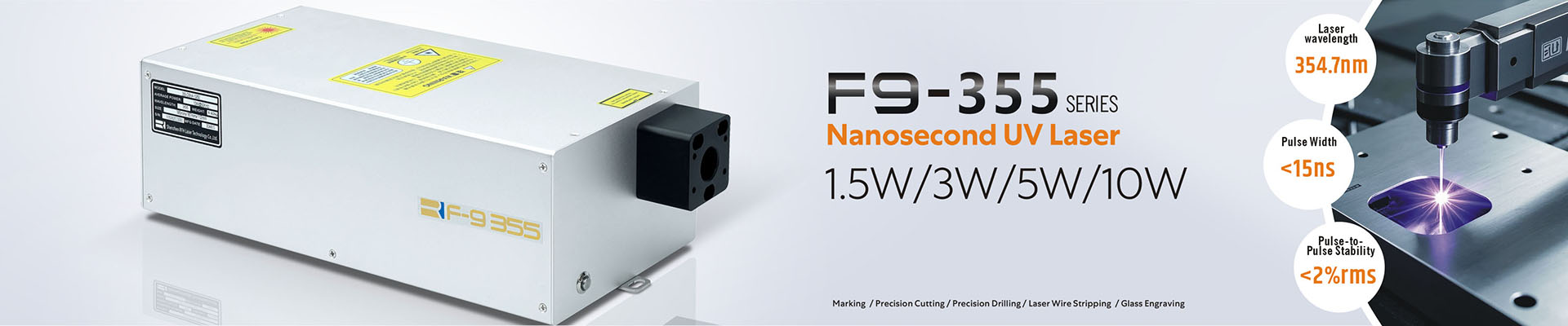
20W/25W Nanosekunden-UV-Laser: höhere Leistung, bessere Wirkung
Wie oben erwähnt, hat die Leiterplattenindustrie meines Landes von der rasanten Entwicklung aufstrebender Industrien wie 5G und Big Data profitiert. Das Aufkommen neuer Industrien und neuer Technologien hat auch höhere Anforderungen an die FPC- und PI-Folienschneidindustrien gestellt. Um eine geringere Karbonisierung und eine schnellere Effizienz zu erreichen, führen Laserunternehmen auch ständig technologische Innovationen ein und erforschen ständig höhere Frequenzen, schmalere Impulsbreiten und höhere Leistungen.