Neuester Blog
Warum sollten Sie sich für das Schneiden von Wafern für eine 10-W-UV-Laserschneidmaschine entscheiden?
Oct 18 , 2021
Most semiconductor materials of ultraviolet laser cutting machine have good absorption of light in the ultraviolet band. Take the absorption of monocrystalline silicon in different wavelength bands as an example. When the semiconductor material is processed by laser in the ultraviolet band, due to the narrow focus spot of ultraviolet light, The photon energy is relatively high and can break the chemical bond of the material. The volume of the space occupied by the product expands rapidly, and finally shoots and separates the parent body in the form of a bulk explosion and takes away the excess energy. The hot zone has little effect. In this process, since there is no heat generated, the process of ultraviolet laser is also called "cold working". After the cutting is completed, each chip is separated by the corresponding split process. In this way, the machine can be used effectively, and at the same time, it can be convenient for us to find the fault in the maintenance of the problem, and facilitate the maintenance.
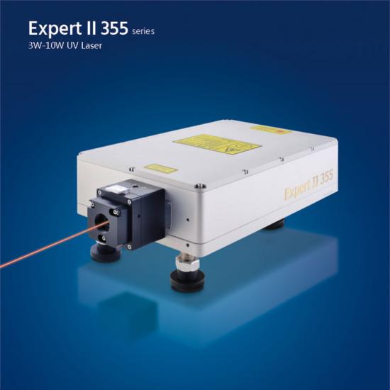
355nm UV laser cutting machine
Because the energy of this special wavelength and frequency laser acting on the material to be processed is only a few watts or even milliwatts, there is no molten material on the outside or inside, and the front and back sides are almost invisible with the eyes. , This provides a larger space for chip manufacturers to reduce the width of the cutting channel and increase the number of chips per unit area to reduce costs. Since the short-wavelength ultraviolet laser has almost no thermal damage, the material does not need to be cooled, and the entire cutting process is performed in a completely dry environment. The molten material is also vaporized, so the appearance of the material is not contaminated at all, which also solves the problem of contamination of semiconductor wafers.

uv laser | green laser | ultraviolet lasers | uv dpss laser | nanosecond laser | UV laser source | Solid State Lasers
The application of UV lasers is becoming more and more popular
At present, with the gradual maturity and stability of ultraviolet lasers, the laser processing industry has shifted from infrared lasers to ultraviolet lasers. At the same time, the application of ultraviolet lasers is becoming more and more popular, and laser applications are moving towards a broader field. The working principle of the UV laser cutting machine is UV laser wafer cutting. The surface of the sapphire substrate is hard. Generally, the cutter wheel is difficult to cut, and the wear is large, the yield is low, and the cutting path is larger than 30 μm, which not only reduces the use area, And it reduces the output of the product. Driven by the blue and white LED industry, the demand for sapphire substrate wafer cutting has increased greatly, and higher requirements have been put forward for improving productivity and finished product qualification rate.
Anwendung von UV-Lasern im Bereich der Halbleiterchipbearbeitung
Tatsächlich umfasst die Anwendung von Ultraviolettlasern im Bereich der Halbleiterchipverarbeitung hauptsächlich: Chipschneiden, Wafer-Mikrolochbohren, Wafermarkierung, Lasereinstellung des Dünnschichtwiderstands, Lasermessung, Laserätzen, tiefe Ultraviolett-Projektionslithographie usw. Um sich in diesen Anwendungen an die kontinuierliche Entwicklung der Großserienproduktion anzupassen, ist die herkömmliche Formtrennungstechnologie aus Sicht der Leistung und der Kosten nicht mehr praktikabel, und die Ultraviolett-Laserschneidtechnologie wird zu einer Anwendung mit großem Potenzial. Die Schlüsseltechnologie der Anwendung. Das macht uns auch noch überzeugter vom Erfolg dieser Technologie.