Mexiko-Kunde kauft 5 Einheiten kompakter UV-Quellen zum Bohren von Mikrolöchern in Leiterplatten
Dec 12 , 2022Mexico customer buy 5 units of compact UV sources for PCB circuit board drilling micro holes
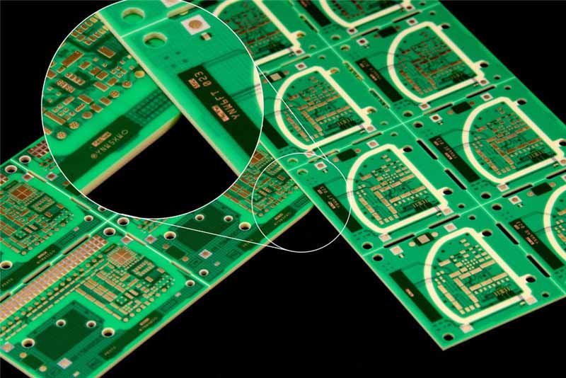
The portability and miniaturization of electronic products is the general trend, which corresponds to the miniaturization and high density of circuit boards. Electronic engineers improve the technical route plan for miniaturization of circuit boards, often by drilling holes with smaller diameters and narrower spacing on the substrate to obtain higher-density wiring space. layout and save space for higher speed, higher density boards.
The designer's wish is always beautiful, but the reality is cruel. First, due to the limitation of the material characteristics of the drill bit, the physical limit that the conventional mechanical drill bit can reach should be 0.10mm-0.15mm, which is equivalent to one-eighth of a human hair, and the manufacturing cost of the drill bit is high; There are requirements for the thickness of the board. Generally, the ratio of thickness to diameter is 1:8, that is, the thickness of the board corresponding to the hole drilled at 0.1mm is generally not more than 0.8mm. In fact, the circuit board has now expanded from single-layer boards to double-layer boards and more complex high- High-precision multilayer board; third, due to the high drilling speed of mechanical drilling, the heat generated is large, which affects the drilling efficiency to a certain extent; fourth, the axial force and cutting torque during mechanical drilling also pose challenges to the drill material , It is a test of the strength and wear resistance of the drill bit.
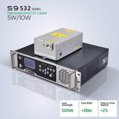
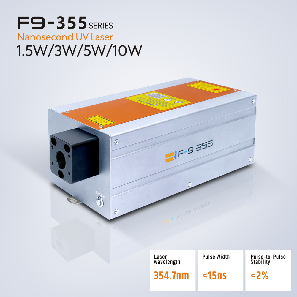
Obviously, conventional mechanical drilling cannot meet the higher requirements of micro circuit boards. As a new type of processing method, the high collimation, high energy density and small spot diameter of the 355nm ultraviolet nanosecond laser can drill holes with high precision, high quality and high processing efficiency on the circuit board, which is in line with the short production time of the current circuit board. The characteristics of cycle and quick response.
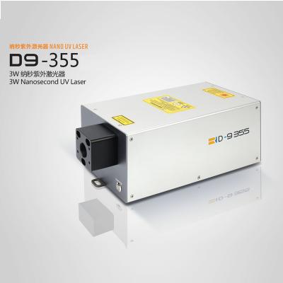
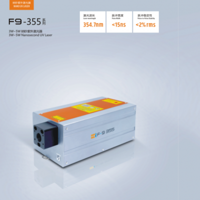
Der 355-nm-UV-Nanosekundenlaser ist derzeit der Mainstream-Laser für die industrielle Mikrobearbeitung. Es hat eine kurze Wellenlänge, eine hohe Materialabsorptionsrate, eine hohe Einzelphotonenenergie und erzeugt beim Bohren keine große Hitze. Diese Art der Verarbeitung wird oft als "kalte" Verarbeitung bezeichnet. , die einfacher ist, eine bessere Bohrwirkung zu erzielen als die Wärmebehandlung von Infrarotlasern. Insbesondere ist die Innenwand des Lochs glatt, die Kantenabsplitterung gering und die Verjüngung klein; Darüber hinaus ist die Strahlqualität dieses Lasers ausgezeichnet (M2 < 1,2) und die Fokussierbarkeit ist gut, der Fleckdurchmesser nach dem Fokussieren liegt in der Größenordnung von Mikrometern (10–20 μm), was die Verarbeitungsanforderungen herkömmlicher Leiterplattenlöcher erfüllen kann auf dem Markt.